How Long Does It Really Take to Go From PCB Design to Final Product?
varsha June 18, 2025 0 COMMENTS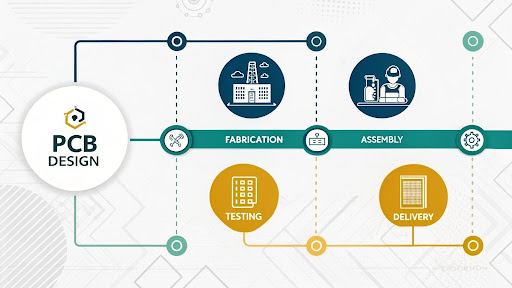
Imagine yourself having just completed your outstanding PCB design, feeling great about your creative circuit, and almost seeing your finished product in your hands. Reality then strikes—how long is the process really going to take? Like most engineers and businesspeople, you are likely wondering whether your completed product will show up in weeks, months, or perhaps even years.
Actually, the path from PCB design to final product is more than just about the PCB itself. This is a complicated dance with several phases, each with a chronology, possible mistakes, and variables that might either greatly hasten or slow down events. Let’s examine the actual chronology and what to anticipate along the way.
Table of Contents
The PCB Manufacturing Phase: Your First Big Turning Point
Actual PCB manufacturing starts once your design files are ready and you have triple-checked everything. Usually, depending on the complexity and your manufacturer’s present workload, standard PCBs call for five to fifteen business days. While complicated multi-layer boards with particular needs might take two to three weeks, simple two-layer boards can often be turned around in just a few days.
On advanced technologies like HDI (High Density Interconnect) boards, however, the timeline can be rather long. For instance, OurPCB HDI PCB production uses more advanced techniques, including microvias and sequential laminating, which naturally call for more time but provide exceptional performance for high-frequency uses.
Most importantly, your PCB manufacturing schedule is defined by:
- Layer count
- Board size
- Surface finish requirements
- Any special materials or techniques
Although they are sometimes available, rush orders come with premium pricing and might not always provide the necessary quality control for your finished goods.
Component Sourcing: The Sometimes Ignored Time Sink
Many people undervalue the timeframe here; component procurement can cause your main bottleneck. Depending on what you need, getting all your components can take anywhere from a few days to several months in the supply chain of today.
You can easily find and ship common parts like resistors, capacitors, and standard ICs within a week. Custom parts, specialized components, or anything with supply chain restrictions could have, however, lead times ranging from 12 to 52 weeks or even more. Recent years’ semiconductor shortage has shown us that even apparently basic chips can be major project roadblocks.
Usually starting early in the design process, even before the PCB layout is finished, smart project managers start component sourcing. In your overall calendar, this parallel approach can save weeks or months. From the start, think about including backup component options in your circuit; it’s far simpler than redesigning later when the desired component isn’t available.
Assembly and Testing: The Product Your PCB Turns Into
Assembly starts when you have all components at hand and your bare PCBs. Electronic manufacturing usually takes three to ten business days for prototype quantities, depending on the complexity of your board and the workload of the assembly house. Production quantities naturally take more time—often two to four weeks for bigger runs.
Among several important steps in the assembly process are:
- Solder paste application
- Component placement
- Reflow soldering
- Several inspection procedures
More complicated boards, including BGAs, special assembly needs, or fine-pitch components, will call for extra time and careful handling.
Testing is the process by which you find out whether your months of designing effort really serve as intended. Initial functionality testing may find problems needing component substitutions, design changes, or assembly rework. Set aside extra time for this phase; it’s rare that everything goes exactly on the first try, and rushing through tests usually results in issues found much later in the process.
The Integration Challenge: Making Everything Work Together
Your PCB doesn’t exist alone frequently. Most products call for mechanical integration, software development, regulatory compliance, and extensive system-level testing. Especially for complicated products, this integration period can easily span several months.
Mechanical integration is designing enclosures and heat management systems and making sure your PCB fits the general product design. While final integration and testing call for functioning hardware, software development for embedded systems sometimes lasts the whole hardware development process.
Not overlooked should be legal requirements as well. Add several extra months to your calendar should your product require FCC certification, CE marking, or other regulatory approvals. These procedures usually call for design changes that return you to earlier phases and cannot be hurried.
Handling Your Timeline Anticipations
What then is the correct response to our first question? After completing the PCB design, the final product for a basic item with standard components may be available in two to four months. More complicated products with unique components, cutting-edge PCB technologies, or strict regulatory needs could readily take six to twelve months or more.
Managing time effectively requires parallel processing wherever feasible. Start component procurement early, start regulatory planning in the design stage, and keep close contact with every one of your suppliers and partners. Plan buffer time for the unavoidable, unanticipated delays.
Strategic Planning for Success
Recall that your first prototype is hardly finished. Most effective initiatives run several times, each needing time for redesign, re-manufacturing, and re-testing. Please consider incorporating this reality into your calendar of events from the beginning.
Most effective project managers view timeline estimation as a risk-management tool. Early on they spot possible bottlenecks, create backup plans, and keep reasonable expectations all through the process.
About to Begin Your Trip?
Although the road from PCB design to final product is not clear-cut, knowing the chronology will help you properly budget and create reasonable expectations. Every project is different; your particular needs will finally decide your timeframe.
How would you describe your experience with PCB-to-product schedules? Have you discovered means to speed the process or come across unanticipated delays? Share your stories in the comments below; the community gains most from our real-world experiences—both the triumphs and the setbacks that provide insightful lessons on routes of action.
RELATED ARTICLES


Latest Articles
 Jagermeister 750ml Price in India: Full …In Whisky Prices
 Building a Scalable Payment Infrastructu…In Technology
 Tech-Savvy Ways to Streamline Your Finan…In Business
 Magic Moments Vodka Price in India: Size…In General
 The Role of Claims Agencies in Holding A…In Tips
 How Embracing Cloud‑Native Strategies Tr…In Technology
 Poorvika Mobiles Pun: Best Place for You…In Technology
 Why Choosing the Right NEET Coaching Mak…In Education